




Choose your country and language
Language

The ability to design and manufacture printed circuit boards (PCBs) is essential for electronics manufacturers because it enables them to create compact, reliable electronic devices.
If you have tried building your own circuit without a PCB, you know the struggle of not really knowing why the circuit is not working as intended. Perhaps there is just too much noise in the circuit or a loose connection somewhere. Who knows? If you are not careful, the circuit might even zap you! Just look at this sad circuit below.

So how do we eliminate these irritating factors from circuit development and make our circuits beautiful and reliable? By using a printed circuit board!
A PCB (printed circuit board) refers to the layout design on a circuit board used to connect electronic components together.
A PCB is typically made of an insulating material (such as fibreglass or plastic) with conductive copper traces etched onto its surface. The copper traces create electrical connections between components mounted on the board.
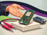
The PCB layout is a visual representation of the circuit board design, showing the location of all components and the routing of copper traces. Once your board is finished, you can connect your components in the circuit as though they were Lego bricks! (Sometimes a little drilling may be required, though.) See how neat and attractive a circuit board can be.

PCB design is an essential part of the manufacturing process because it serves as the blueprint for developing the physical board. Once a PCB layout is finished in a program, it is used to create the circuit board through a process involving etching away excess copper and drilling holes for components to be mounted. In a sense, the PCB design is printed on a special printer.
This is the step where we move from theory, including the maths and simulations for our circuit, to practice. We may have done all the maths correctly and even drawn our circuit perfectly in the simulation program and tested for the correct voltages and currents, BUT this does not ensure it will work perfectly when we assemble the circuit in real life.
In fact, there are quite a few things to consider. Let’s go through some of them.
Component Placement
The placement of components on the PCB must be carefully considered to ensure they are correctly positioned and spaced. Components that generate heat, such as microcontrollers or power regulators, should be placed in areas with good airflow to prevent overheating.
Trace Routing
Trace routing on the PCB must be designed to minimise electrical noise and signal interference. These traces should be kept as short as possible and avoid crossing each other to prevent crosstalk.
Power and Ground Planes
Power and ground planes can be incorporated into the PCB design to provide stable power and reduce noise. The power and ground planes should be as close to the components as possible and each plane should connect to the components’ corresponding net through suitable vias for a low-impedance path. Power and ground must not be shorted together.
Signal Integrity
PCB design must account for signal integrity to ensure signals do not deteriorate as they travel through the board. Factors such as trace impedance, signal reflection and termination should be considered.
PCB Layer Stack-Up
The number and arrangement of layers in the PCB can affect board performance. The PCB stack-up should be designed to minimise electromagnetic interference (EMI) and ensure sufficient room for routing and component placement. Electromag-what? See this blog to learn about electromagnetism!
Design for Manufacturability
The PCB design should be optimised for production, taking into account the PCB manufacturer’s capabilities and limitations. This includes factors such as board size, minimum trace width and spacing, drill sizes and copper weights.
Language
